PROJECT OVERVIEW
As part of Georgia Tech’s Advanced Packaging course, I contributed to a multi-stage fabrication and reliability assessment process for glass core-based advanced IC packaging, involving through-glass via (TGV) drilling, die embedding, ABF dielectric build-up, seed layer sputtering, photolithography, electroplating, and warpage testing.
KEY CONTRIBUTIONS & TECHNIQUES
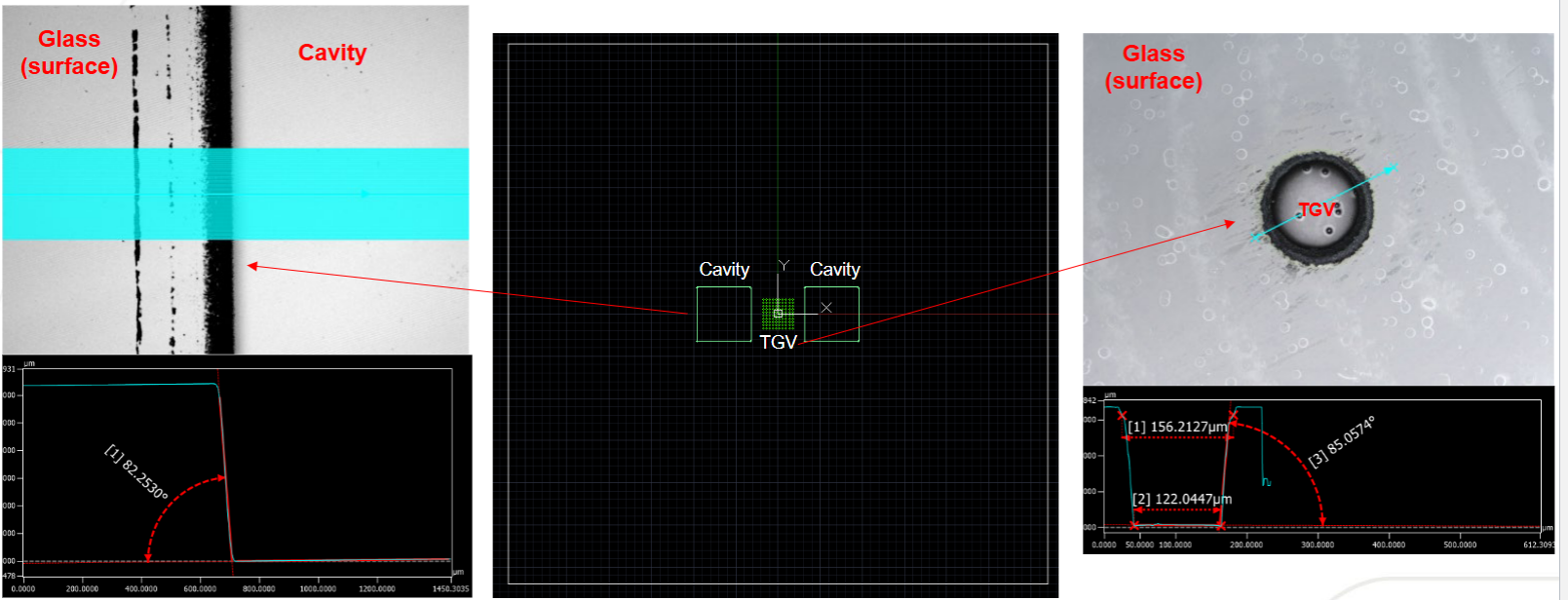
LASER ABLATION OF TGVs
- Used femtosecond IR laser to fabricate high-aspect ratio through-glass vias for IC embedding with sub-85° taper quality—meeting edge fidelity criteria critical for resin flow and mechanical anchoring.
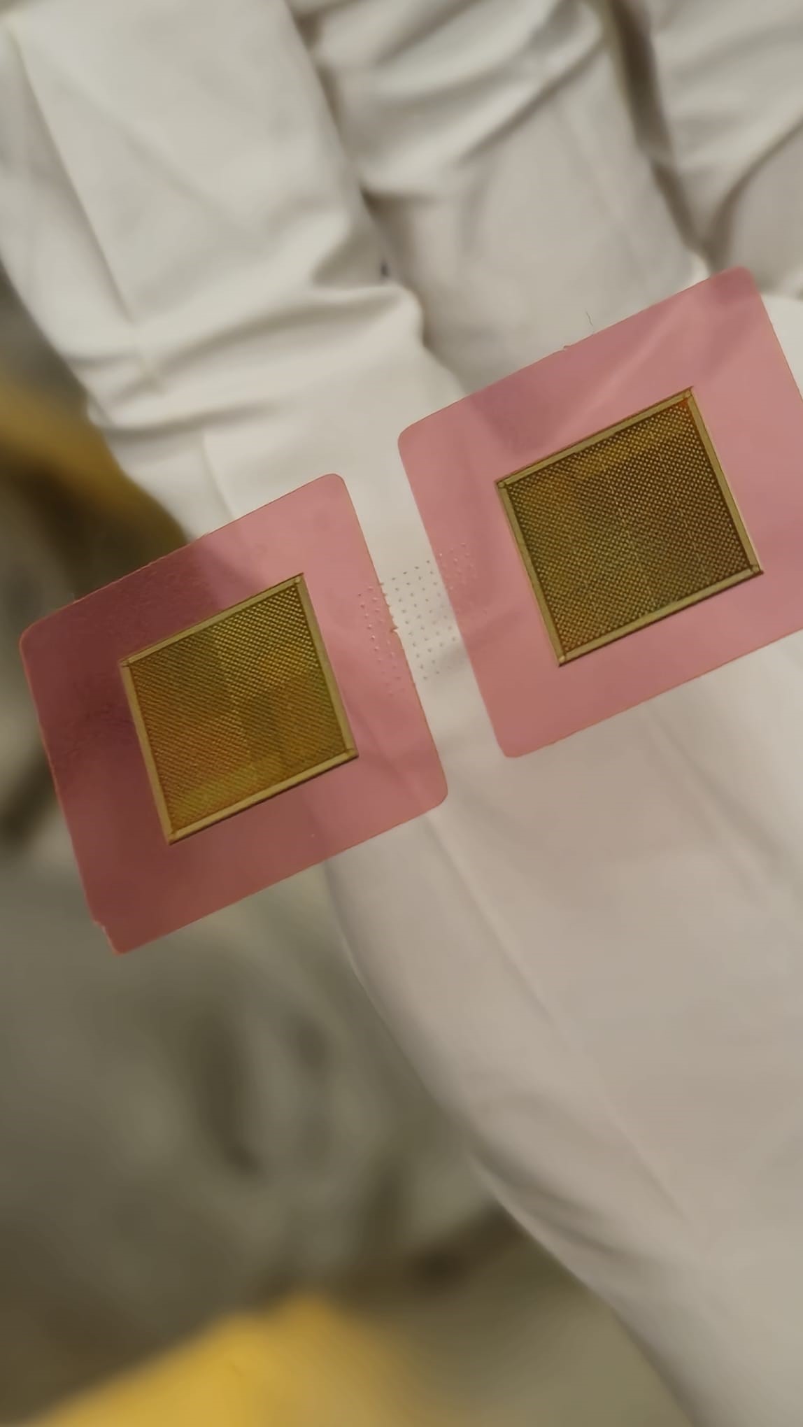
DIE EMBEDDING & ABF PROCESSING:
- Embedded IC dies into ablated cavities using thermal release tape and FINEPLACER machine; applied ABF GL-102/107 layers to encapsulate dies, simulating high-density multi-die packaging.
SURFACE PREPARATION & SEED LAYER METALLIZATION:
- Modified ABF surface using oxygen plasma (Oxford RIE) and sputtered Ti/Cu seed layers via Denton Discovery, forming reliable metal-dielectric interfaces crucial for next-gen substrate interconnects.
PHOTOLITHOGRAPHY WITH MASKLESS ALIGNER:
- Patterned interconnect features using Heidelberg MLA300 system; developed 3 µm TOK photoresist for fine feature definition (~1.5 µm resolution), suitable for sub-10 µm line/space applications.
ELECTROPLATING & OVERPLATING MANAGEMENT:
- Performed copper electroplating into patterned trenches while ensuring thickness control below PR height to avoid shorting—verified using profilometry and post-process strip/etch analysis.
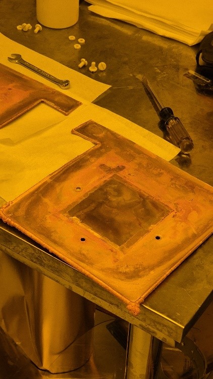
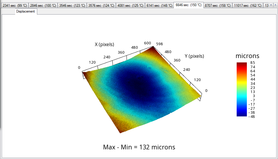
THERMOMECHANICAL RELIABILITY TESTING:
- Evaluated package warpage via shadow moiré interferometry; confirmed ABF/glass CTE mismatch and asymmetric layering as key drivers of concavity and bowing under thermal cycling (RT–250°C).
TOOLS & TECHNOLOGIES
- Packaging Tools: Heidelberg MLA300, FINEPLACER Matrix, Denton Sputterer, Oxford RIE, Shadow Moiré Interferometer
- Processes:Laser micromachining, vacuum lamination, dry & spin coating, plasma surface prep, electroplating, photolithography
- Materials: ABF GL-102/107, TOK PR, Ti/Cu seed stack, NMP stripper, thermal release adhesives
- Technical Skills: Semiconductor packaging, maskless lithography, interconnect metallurgy, thermal warpage characterization