PROJECT OVERVIEW
With the rise of high-performance, miniaturized electronics, ultra-fine pitch flip-chip assemblies using glass core substrates are emerging as next-generation packaging solutions. However, these structures face major thermomechanical reliability challenges—primarily fatigue failure of solder joints under cyclic thermal loading.
To address this, we developed a detailed finite element modeling (FEM) framework focused on Level 1 assembly (die-on-glass) using a 50 μm solder bump pitch. Our simulation methodology integrates material-level viscoplasticity, parametric design variation, and fatigue life prediction to identify failure modes and propose design mitigation strategies.
FAILURE MODE & RISK CONTEXT (FMEA-Informed Framing)
Failure Mode
Low-cycle fatigue at solder joints due to plastic strain accumulation
Root Cause
CTE mismatch between silicon, glass, underfill, and solder materials
Effect
Cracking at die corners → electrical disconnect → long-term failure
Risk Level (RPN)
135 (High) = Severity (9) × Occurrence (5) × Detection (3)
Detection & Mitigation
Detection: FEM simulation (ANSYS), Anand viscoplastic modeling, validated via corrected Suhir model
Mitigation: Parametric FEM analysis on glass thickness and underfill coverage
TECHNICAL APPROACH
FATIGUE ANALYSIS
- Accumulated plastic strain extracted from stabilized cycles
- Fatigue life estimated using: Kanchanomai model and Andersson model
- Conservative design chosen by selecting lower of the two predictions
MATERIAL BEHAVIOR
- SnAg solder modeled with Anand viscoplasticity
- Copper: bilinear isotropic hardening
- Glass, silicon, ABF-Cu, underfill: temperature-dependent elastic models
- Thermal cycling from –55°C to 125°C applied over 11 cycles (JEDEC JESD22-A104 Condition B)
GEOMETRY & MODELING
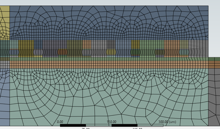
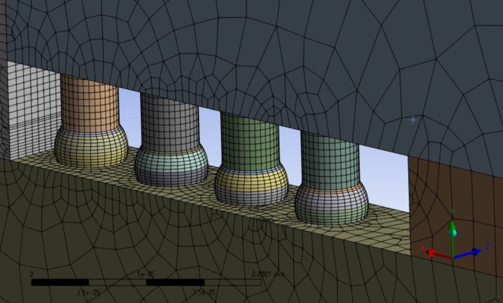
2D plane strain model of diagonal flip-chip cross-section
- 2D plane strain model of diagonal flip-chip cross-section
- Shared topology meshing for accurate stress continuity
- Fine mesh at solder joints to capture stress gradients
- PLANE183 elements used for nonlinear plasticity and viscoplastic behavior
PARAMETRIC DESIGN OPTIMIZATION
VARIABLES STUDIED
- Glass thickness: 200 µm, 300 µm, 400 µm
- Underfill coverage: None, Half Fillet, Full Fillet
FINDINGS
- Stress trend: Non-linear; peaks at 300 µm then slightly decreases
- Deformation trend: Monotonically decreases with thicker glass
- Fatigue life: Best case at 400 µm glass + half underfill (Nf ≈ 2,494 cycles)
Optimization Results
| Configuration | Δε (%) | Cycles to failure (Kanchanomai) | Cycles to failure (Andersson) |
|---|---|---|---|
| 200 µm, no underfill | 1.95E-2 | 1,908 | 2,002 |
| 400 µm, half underfill | 1.67E-2 | 2,249 | 2,494 |
| 400 µm, full underfill | 1.73E-2 | 2,173 | 2,381 |
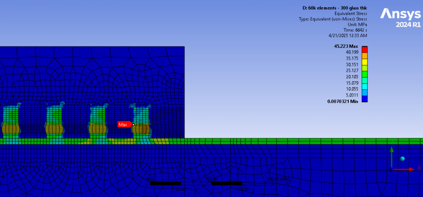
Non-linear stress trend with varying glass thickness
IMPACT
This study offers a validated simulation-based strategy to guide the design of reliable, high-density flip-chip assemblies for next-gen electronics. It pinpoints material and structural interactions that contribute to premature failure and proposes physically grounded optimizations to extend device lifespan.
From a systems engineering perspective, the work also provides a risk-reduction framework that integrates failure identification, sensitivity analysis, and simulation-validated design tradeoffs—critical for manufacturable, robust packaging solutions.
FUTURE WORK
- Extend to 2.5D and 3D models for improved Z-axis accuracy
- Investigate arc fillet profiles and organic substrates
- Study standoff height variations and multi-layer ABF effects
- Perform board-level FEM modeling (Level 2 assembly)
- Correlate results with experimental data from thermal cycle tests